


Editor: Jin Jie
Doc. Version: 2018.07.18
Doc. Category: Maintenance Guide
Content of This Doc.: mainly about the fault checking and hash board tester pinpointing of Antminer L3+.
※ The copyright of this article belongs to Bitmaintech Pte.Ltd. (Bitmain). The article shall solely be reprinted, extracted or used in any other ways with the permission of the copyright owner. Please contact Bitmain official customer service if there is any need of reprinting or quoting.
I. Maintenance Platform Requirements
1. Thermostat soldering iron at 350-450 degrees Celsius, pointed solder tip for small patches like r-c.
2. Heat gun for chip disassembly and soldering, no long time heating in case of PCB blistering.
3. APW3 power source with 12V and 133A Max output to test the hash board.
4. Multimeter, tweezer, L3+ hash board tester (oscilloscope preferred).
5. Scaling powder, cleaning water and anhydrous alcohol; cleaning water is used to clean the residue and appearance after maintenance.
6. Tin grinder, tin stencils, and tin cream; implant tin for chips upon renewals.
7. Heat-Conducting Glue, black (3461), to glue cooling fin after maintenance.
II. Maintenance Requirements
1. Maintenance Personnel in possession of good electronics knowledge, 1 year+ experience and sound mastery of QFN encapsulation and soldering techniques.
2. Check more than two times after maintenance and the result of each time is OK!
3. Watch out for the techniques used, make sure of no obvious PCB deformation after changing any fittings, check for missing/open circuit/short circuit on parts.
4. Check the maintenance target and corresponding test software parameter and hash board tester.
5. Check the tools and testers.
III. Principle and Structure
● Principle Introduction
1. L3+ has 12 voltage domains connected in series, each domain has 6 BM1485 chips, and the entire board has 72 BM1485 chips.
2. BM1485 chip has built-in voltage-reduction diodes, decided by designated pin of the chip.
3. L3+ has 25M monocrystal oscillator on the clock, connecting in series and passing on from the 1st chip to the last chip.
4. L3+ has independent cooling fins on the back of each chip. SMT paster on the front and the one on the back was fixed on the back of the IC by heat conducting glue after initial testing. Upon completion of every maintenance, it has to be fixed by black heat conducting glue (evenly distributed) on the back of the IC.
If you have certain maintenance knowledge, when your Antminer L3+ fails, you can purchase the necessary maintenance tools and accessories to repair the L3+ miner yourself, so as to reduce the profit loss caused by the miner failure.
Necessary maintenance tools and spare parts:
ANLIXIN-862D desoldering station
Antminer thermosetting adhesive
● Key Point Analysis:
1.Below is the signal flow diagram of L3+ signal panel:
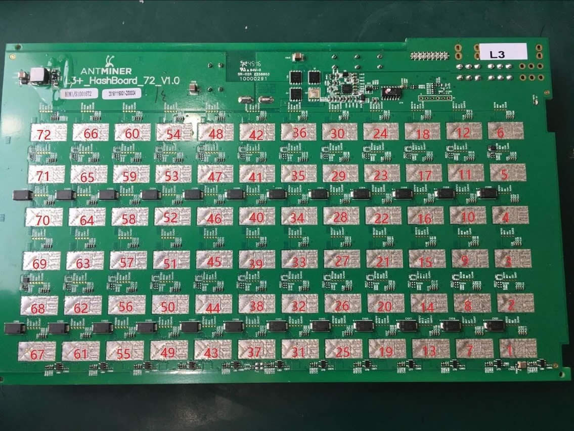
Fig 1. Signal Flow
CLK signal flow, produced by Y1 25M crystal oscillator, transmits from No. 1 chip to No. 72 chip; in standby and computing, both the votalges are 0.9V. TX (CI, CO) signal flow, IO mouth pin 11 in, transmits from No. 1 to No. 72 chip; the voltage is 0V when IO wire is not plugged, and the voltage is 1.8V in computing.
RX (RI, RO) signal flow, returns from No. 72 to No. 1 chip, and then returns to control panel from IO mouth pin 12; the voltage is 1.8V when IO signal is not plugged, and the voltage is also 1.8V in computing.
B (BI, BO) signal flow, lowers electrical level from No. 1 to No. 72 chip; the voltage is 0V when IO wire is not plugged or in standby, and the singal impluse is about 0.3 in computing.
RST singal flow, IO mouth pin 15 in, transmits from No. 1 to No. 72 chip; 0V when IO signal is not plugged or in standby, and 1.8V in computing.
2. Below shows the critical circuits on the front of L3+ hash board.
1) Testing points among chips (as below after amplification): Fig 2
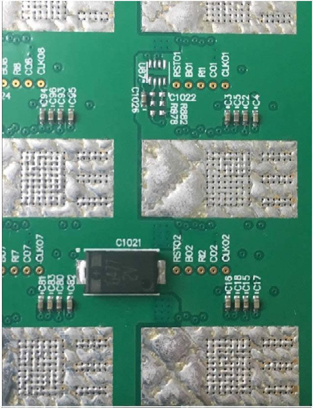
Fig 2. Testing Points among Chips
In Maintenance, testing the testing points among chips is the most direct fault-locating method. The arrangement of L3+ hash board is as the following: RST, B0, RI (RX), C0 (TX), and CLK signal.
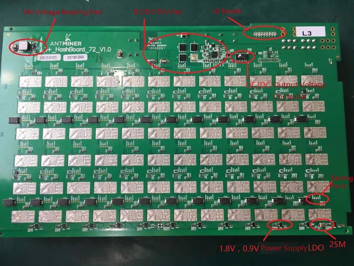
Fig 3. The Critical Circuits on the Front of hash board
2) Voltage Domain: the entire board has 12 voltage domains, and each domain has 6 chips. The 6 chips in the same voltage domain are in parallel power supply, and then connect other voltage domains in series. The circuit structure is as below Fig 4:
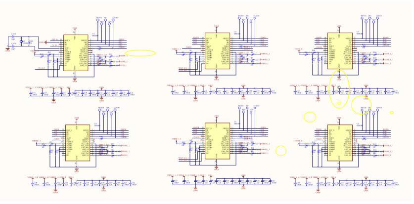
Principle Analysis of Voltage Domain Single Chip (see below Fig 5 and Fig 6):
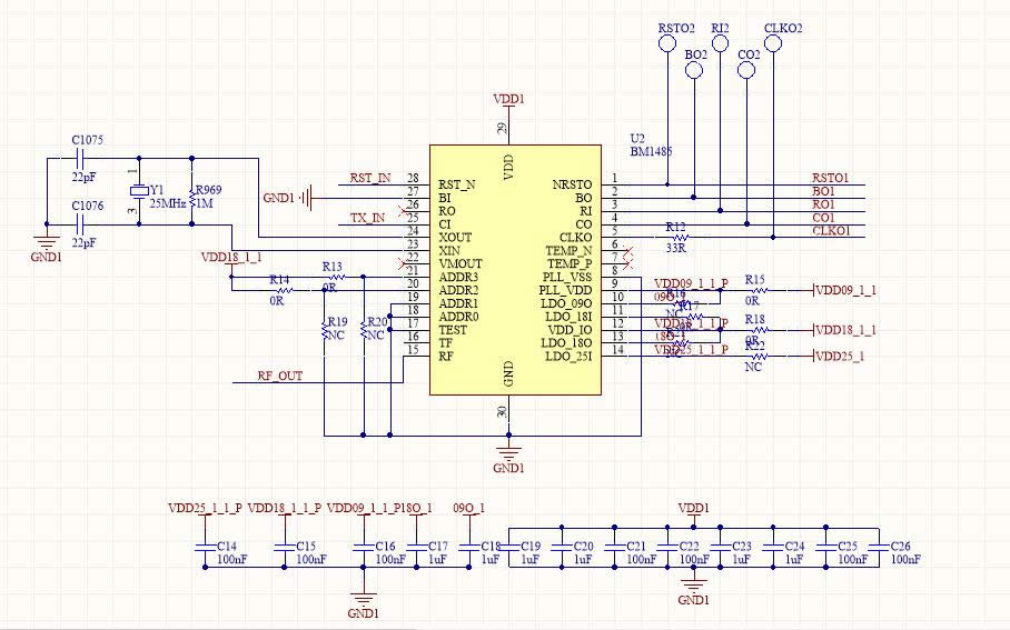
Fig 5. BM1485 Circuit Diagram
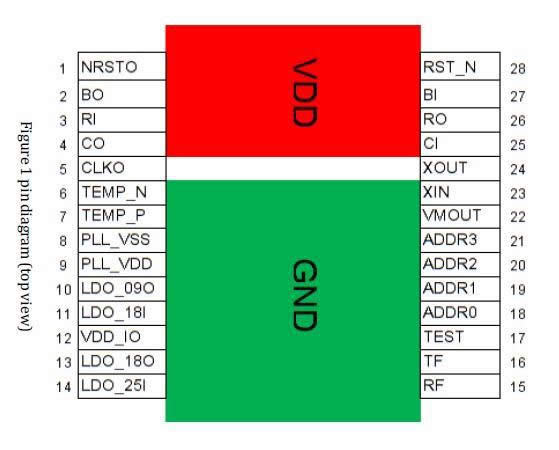
Fig 6. BM1485 Chip Pins
● The above is the pin functions of BM1485 chip.
In maintenance, mainly test the ten testing points on the front and back of chip (front and back have 5 respectively: CLK, CO, RI, BO, RST); CORE voltage: LDO-1.8V, PLL-0.9V, DC-DC output, and booster voltage 14V.
Test Methods:
1) When IO wire is not plugged and only 12V is plugged: DC-DC output is 10V or so, and booster voltage output is about 14V. Among testing points, CLK must be 0.9V, RI must be 1.8V, and the voltage of others must be 0V;
2) When IO wire is plugged and test key is not pressed, DC-DC and booster voltage have no voltage output; when tool test key is pressed, PIC begins to work. At that moment, DC-DC outputs the voltage set up by tool test program, and booster voltage begins to work. Then tool outputs WORK, and hash board returns nonce after computing. This moment the normal voltage of each testing point should be:
CLK: 0.9V
CO: 1.6-1.8V. When tool just sends WORK, CO is negative polarity, so DC level will be lowered and the transient voltageis about 1.5V.
RI: 1.6-1.8V. In computing, anomaly voltage or low voltage will cause hash board anomaly or zero hash rate. BO: 0V when there is no computing; and 0.1-0.3V impulse beat in computing.
RST: 1.8V. Every time when pressing tool test key, output reset signal again.
When any testing point status or voltage is abnormal, infer fault point according to the circuits before and after the testing point.
●It can be seen from above list:
CLK signal: Pin 23 in, Pin 5 out, when crossing domains, Pin 5 out, via a 100NF capacitor, enters the Pin 23 of the next chip.
TX signal: Pin 25 in, Pin 4 out;
RX signal: Pin 3 returns, Pin 26 out;
BO signal: Pin 27 in, Pin 2 out;
RST signal: Pin 28 in, Pin 1 out.
Test each signal voltage, CORE voltage, LDO-1.8OV, PLL-0.9V, etc. of chip:
CORE: 0.8V — generally the chip CORE short circuit of this voltage domain will cause this voltage anomaly.
LDO-1.8O: 1.8V — LDO-1.8O short circuit or open circuit of this chip will cause this voltage anomaly.
PLL-0.9: 0.8V — PLL-09V power supply short circuit of a chip of this voltage domain will cause this voltage anomaly.
3) Determine the operation condition of hash board, hash rate of chip, the sense of heat, etc. according to the printwindow information of tool.
3. IO Mouth: IO is composed of 2X9 pitch 2.0 PHSD 90°dual inline package. The definition of each pin as below Fig 8:

Fig 8. Each Pin Definition of IO Mouth
As shown in above Fig:
Pin 1, 2, 9, 10, 13, and 14: GND.
Pin 3 and 4 (SDA, SCL): the I2C bus wire of DC-DC PIC, connect control panel to communicate with PIC; through which control panel can read and write PIC data, and thereby control the running state its hash board.
Pin 5 (PLUG0): identification signal of hash board, this signal raises 10K resistance to 3.3 V by hash board,
so this pin is high level when IO signal is plugged.
Pin 6, 7 and 8 (A2, A1, A0): PIC address signal.
Pin 11 and 12 (TXD, RXD): hash rate channel of hash board 3.3 end, and changes into TX (CO), RX (RI) signals through resistive voltage division; the electrical level of all IO mouth pin ends is 3.3V, and changes into 1.8V through resistive voltage division.
Pin 15 (RST): reset signal 3.3V end, and changes into 1.8V RST reset signal through resistive voltage division
Pin 16 (D3V3): hash board 3.3V power supply, this 3.3V is powered by control panel, and mainly supplies working voltage to PIC

The voltage of TX_IN is 1.8V
The voltage of RST_IN is 1.8V
4. 14V Boosted Circuit:
The responsibility is to boost DC-DC (10 - 10.4V) to 14V, and the principle is to boost 10V to 14V through U111 RT8537 switching power supply, the switching signal produced by U111 stores energy via L1 inductance, and then D100 boosted rectifying diode charges and discharges for C1072, and thereby get the 14V of C1072 positive electrode. See Fig 11 and Fig 12:
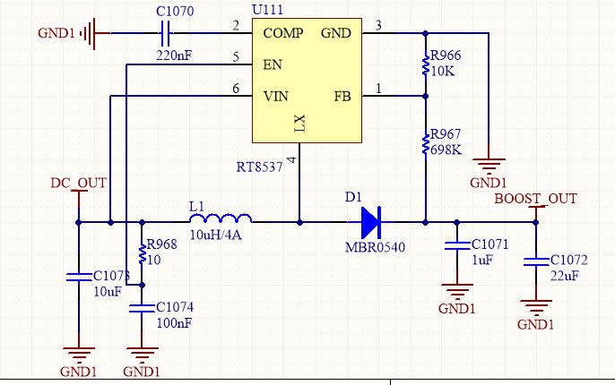
Fig 11. 14V Boost Schematic Diagram
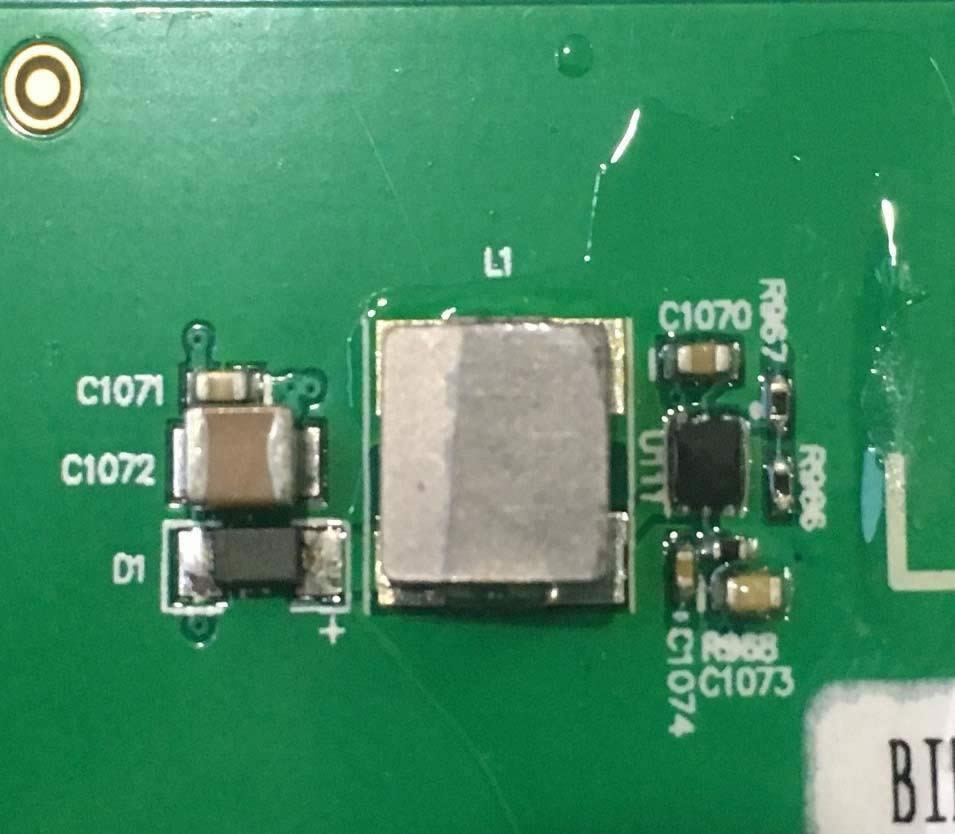
Fig 12. 14V Boost PCB Diagram
Note: the voltage anomaly of boosted circuit often causes the LDO damage of the last 4 voltage domains of hash board, and also causes chip damage easily. And the anomaly of boost voltage is often caused by the oxidation of U111, R996 and R997.
5. DC-PIC: Composed of PIC16(L)F1704. See Fig 13 and Fig 14, the device stores chip frequency information and voltage value of hash board, through which we can control the DC-DC output voltage of hash board.
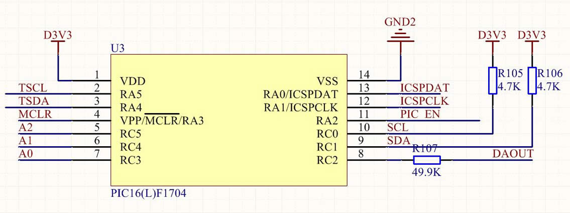
Fig 13. PIC Schematic

6. DC-DC Circuit: Composed of LM27402SQ and CMOS tube TPHR9003NL. See below Fig 15 and Fig 16:

Fig 15. DC-DC Schematic Diagram
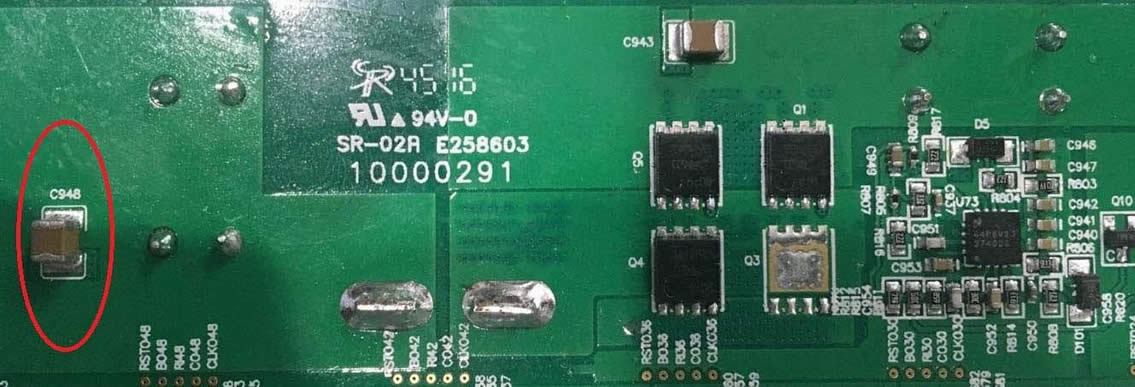
Fig 16. DC-DC Circuit
DC-DC output voltage testing points are the two ends of capacitance C948
When the voltage of DC-DC is abnormal, firstly check the consistency of voltage value of PIC and DC-DC output voltage through tool print information; if they are inconsistent, replace the low capacitance around LM27402SQ;
If DC-DC has no output, check whether the EN voltage of R13 and R14 is 1V or so, the voltage of R11 is 12V, PIC is in normal operation, or PIC can receive 12C signal of control panel normally.
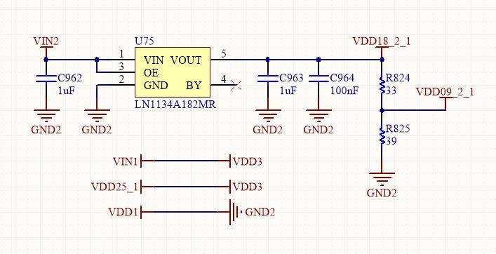
7. 1.8V-LDO: Composed of 1.8VLDO SPX5205M5_L_1_8.
See below Fig:
SPX5205M5, Pin 1 and 3 in, Pin 5 1.8V out
PLL-0.9V voltage is from LOD-1.8 via voltage division of two resistances.
8. Temperature sensor circuit:
Composed of sensor IC, temperature sensor chip passes the Pin 6, 7 of BM1485, collects BM1485 built-in temperature sensor, and finally passes the Pin 15, 16 of BM1485, and returns to the FPGA of control panel via RI. The principle is as Fig 21:
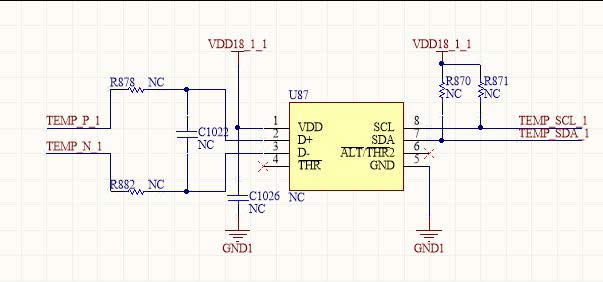
Fig 21. The Schematic Diagram of Temperature Sensor
IV. Maintenance Process
● Sample:

1. Regular Check: observe the target board to find cooling fin displacement, deformation or burn? Such issues take priority, displacement can be solved by taking it off, wash off the glue and re-glue it after the maintenance.
If there is no problem, then check impedance of each and every voltage domain to see if there is short/open circuit, which then takes priority.
Check if every domain reaches 0.8V and voltage different no greater than 0.05V. Voltage too high or too low suggests anomalies in the neighboring domains.
2. After Regular Check ( in which short circuit check is a must, in case of burning chips or other fittings when power is on), check the chip with test boxes, judge and pinpoint based on such result.
3. Based on the test box results, check test point from the malfunctioning chip, (CLK IN OUT/TX IN OUT/RX IN OUT/B IN OUT/RST IN OUT), and
VDD, VDD0V8, VDD1V8, etc.
4. Then based on that the signal flows, apart from RX, transmit reversely (No.72 to No.1), and that of signals CLK, C0, B0, RST transmit forwardly (No.1 to No.72.), so the anomaly can be identified with power sequence.
5. When pinpointed the malfunctioning chip, re-solder the chip: add scaling powder around the chip, heat the chip pin to dissolved state, move and press the chip lightly; have the chip pins and soldering pans re-grinded, finish.
Note that if re-soldering do not help, the chip should be changed directly.
6. Run twice with test box on fixed hash board. Test timing: first time should be after changing fittings, with cooled board. The second time should be in a few minutes with fully-cooled board. The gap between two tests will not affect working. Put aside the repaired board and continue with another one, come back to the first one with the fixed second one.
7. Log the malfunction type after maintenance, esp. the model, location and reason. This will further improve the feedback to production, CS andR&D.
8. Conduct formal burn-in after logging.
V. Malfunction Types
Typical malfunctions:
1. Imbalanced impedance among multiple voltage domains: when the impedance of certain domains is deviated from the norm, the anomaly domains could comprise open/short circuits. It is most likely that the chips are the cause. But there are 3 chips in each voltage domain; the problem could be with only one of them. Check and compare the earth impedance of each test point on chips to find the anomaly point and thus locating the problemchip.
Short Circuit: remove the cooling fin from the chips in the same voltage domain, and observe chip pin to spot bridging issue. If you cannot find short circuit point by observing, find it by resistivity method or interception method.
2. Imbalanced voltage among domains: voltage too high or too low suggests IO signal malfunction in the anomaly domain or the neighboring domain. This cause the next domain to show abnormal status and then: voltage imbalance. Check the signals and voltages in test points to find the anomaly point. Some of the cases may require you to compare the impedance among multiple test points to find the anomaly.
Pay special attention: CLK signal and RST signal — anomalies of these 2 are most frequently causing voltage imbalance.
3. Missing chips: missing chips means that when conducting test box checks, all 72 chips cannot be found, but only some of them. The actually missing (cannot find by checking) anomaly chips are not in the shown location. You need to pinpoint the anomaly chip by testing.
The pinpointing can be conducted by intercepting TX. Pivot the TX signal of a certain chip over the land, such as, after setting the TX output of chip no.50, over the earth and all previous chips are normal, the test box should show chip No. 50. If not, the anomaly exist before No. 50; if it does, the anomaly chip is after No.50. Repeat this until you locate the anomaly chip.
4. Broken link:
Broken links are similar to missing chips. The difference is that not all missing chips are in anomaly, but only one abnormal chip causing the following chips to fail. Such as, a certain chip is functional, but it does not transmit information from other chips; this signal chain will be broken right here---this is called broken link.
Test box are capable of showing broken links. Such as: when checking chips, test box report only 14 chips; test box cannot start running until it detects pre- set number of chips, so it only shows the number of chips found. Based on the number “14”, check the voltage and impedance at test points right before and after chip No. 14 will help you to locate the problem.
5. No running:
No running means the test box cannot detect the chip information of the hash board, and shows “No hash board”; this is the most frequent problem,
1) Voltage anomaly of a certain voltage domain: check the voltages among multiple domains to locate the problem.
2) Chip anomaly: check signals among test points to locate the anomaly.
CLK signal: 0.9V, signal is from chip No.1 to No.72. But the current edition offers only 1 crystal oscillator, abnormal LCK causes all subsequent signals to show anomaly. Find the target in the sequence of signal transmission.
TX signal: 1.8V, this signal is from chip No.1, 01...72, look for previous ones when you hit anomaly at a certain point via the method of bisection.
RX signal: 1.8V, this signal return from No.72...1, identify the malfunction reason by checking signal direction. When no running happens to S7 and S9 hash board, this signal takes priority, check it first.
BO signal: 0V, this signal means that when the chip detects Ri return signal in a normal state, it can be pulled to high level, otherwise it should be low level.
RST signal: 1.8V, when the board is powered on and plunged in IO signal, this signal will transmit from 01…72 and till the last chip.
3) Caused by a certain chip VDD
Check the PD (potential difference) among multiple domains. In normal conditions, when the VDD voltage is 0.8V, and the voltage of each test point of other voltage domains is 0.8V as well, the balance among multiple domains is guaranteed.
4) VDD1V8 voltage anomaly of a certain chip
Check the test points of voltage domains to determine whether a certain VDD1V8 is normal or not. Generally, IO voltage determines the voltage of test points. So when the IO voltage is 1.8V, the test points have a normal voltage of 1.8V.
5) Caused by Buck and Booster Circuit Anomaly
Check the two ends of C948 capacitor output (up-left) and see if the voltage is between 10V and 10.4V. Those who are not in the scope may be in need of a re-upgrade to the U3 PIC; make sure the PIC voltage is normal, check to see if U111 has an output of 14V; also check the un-checked peripheral parts and U111 per se.
6. Low hashing:
Low hashing can be divided into:
1) Test box shows NG due to insufficient Nonce and low hashing. The serial port shows information on the number of nonce each chip returns. Generally if the nonce number is lower than the pre-set value, you should look for chip malfunction. If it’s not due to poor soldering or peripheral reasons, you should just replace the chip.
2) Test box shows normal status, but after installation the hashing is low. This is generally due to poor cooling of the chips. Pay special attention to the cooling fin glue, and the general ventilation. Another reason could be that the voltage of a certain chip is critical, and after installation, the 12V power supply is different from the test power supply, thus together resulting in a difference between test hashing and actual running hashing. Tune down and test with the test box, esp. with the DC adjustable 12V power supply. Find the voltage domain that returns the minimum number of nonce.
7. NG of a certain chip:
Means that when testing with the test box, the port information shows the nonce is insufficient or zero of the return of a certain chip. If it’s not due to poor soldering or peripheral reasons, just replace the chip.
● Maintenance Notes
1. The operator should be familiar with the function, flow direction, normal voltage and earth impedance values of each test point.
2. The operator should be familiar with chip soldering to avoid PCB blistering, deformation or pin damage.
3. BM1485 chip is packaged with 14 pins on both sides. Make sure of the polarity and coordinates when soldering.
4. When replacing the chip, clean all the heat-conducting glue on the chip to avoid IC poor soldering or poor cooling (which causes second-time chip damage).