


Guía de reparación de la tablero hash de Whatsminer M10 [EN]
M10 Maintenance Instructions
Table of Contents
1. M10 miner disassembly and assembly
2. M10 chip pin function
3. M10 hash board signal process
4. Introduction to the interlayer, resistance and test points of the hash board
5. Repair methods and cases
1. M10 miner disassembly and assembly
1.1. Disassemble the power supply:
①Pull out the plug of the air outlet fan first, ②Remove the 6 screws on the output end of the power supply, ③Remove the 4 screws fixing the power supply, ④Finally take the power supply out parallel to the direction of the air outlet fan. (Note: It is forbidden to lift the power supply upwards, it will easily deform the positive and negative copper bars. )
1.2. Power supply:
①First install the power supply output terminal parallels to the positive and negative copper bars and align the power supply with the screw holes of the positive and negative copper bars. ②Connect the 4 fixing screws to the power supply, first do not tighten, ③then screw on the copper bar, and fix it on the power output terminal. ④Finally tighten the power supply fixing screw and insert the fan cable.
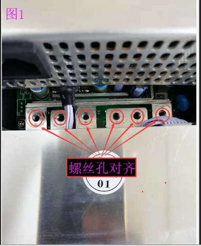
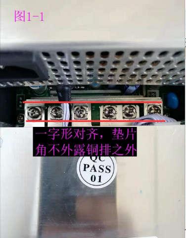
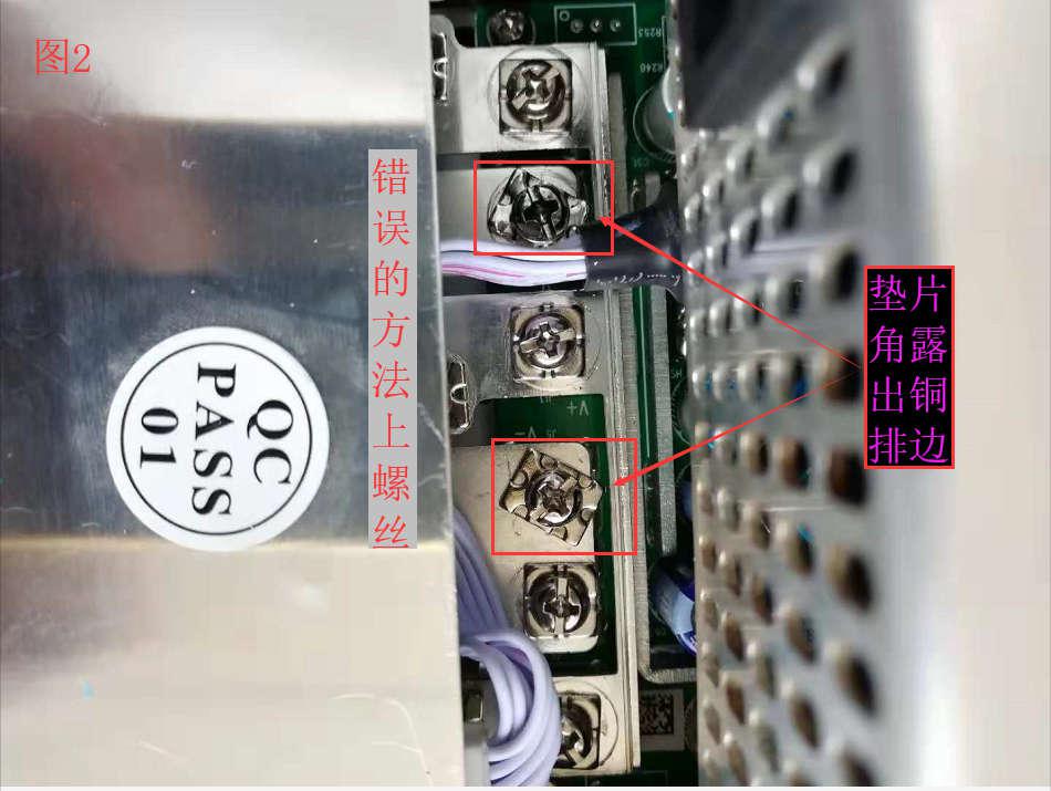
The power supply is installed. (Note: The gaskets of the power terminal screws must be aligned in a straight line, and the corners of the gaskets must not be exposed outside the positive and negative copper bars. ) Correctly tighten the screws as shown in Figure 1 and Figure 1-1, wrong screw as shown in figure 2
1.3. Remove the control board
①Pull out the fan plug of the air inlet first. ②Remove the 4 screws of the control board cover, then move it out a bit, press the cable buckle to pull out the control board power control line, ③Turn the control board cover up to the power supply end, hand hold both sides of the cable plug and gently shake it to pull it out. ④Remove the 4 screws on the control board.
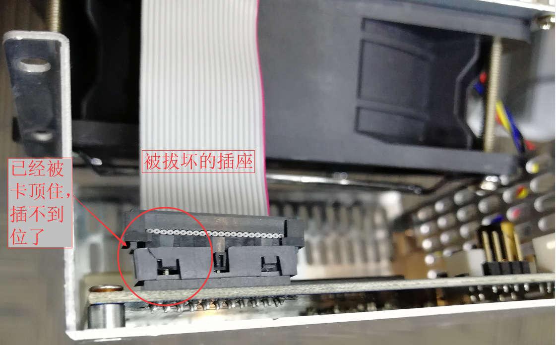
The control board can be removed. (Note: Remember not to pull out the cable, and not more than 15° when shaking gently, otherwise it will be damaged as shown in the figure below)
1.4. Install the control board
①Install the control board on the control board cover, lock 4 screws, ②Insert the cable on the adapter board, insert it tightly and insert it in place, ③Insert the control board power control cable, and insert it in place. ④Lock the screws of the control board cover, ⑤Plug in the fan cable, and insert it firmly, the control is installed.
1.5. Remove the adapter board
①Remove the control board as described in 1 .3 above. ②Remove the control board and cover as a whole. ③Remove the 2 screws on the adapter board. ④Hold the socket with your left hand, and your thumb against the edge of the board, hold the right end of the adapter board with your right hand, shake it gently and pull it up to remove the adapter board.
1.6. Install the adapter board
①Remove the air inlet fan, and remove the fan baffle at the same time. ②Align the male socket of the hashrate board and insert the adapter board, Incorrectly inserted, and press it into place (as shown in Figure 1) method (Figure 2, Figure 3), ③Lock the 2 screws of the adapter board, ④Install the control board as described in ②③④⑤ of 1 .4 above to complete.
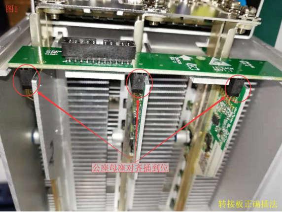
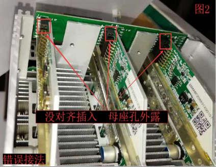
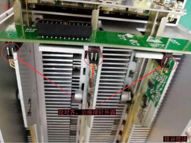
1.7. Dismantling the power board
①Remove the control board as described in 1.3 above. ②Remove the adapter plate as described in ②③④ above 1.5. ③Remove the air inlet fan and remove the fan baffle at the same time. ④Remove the power plate copper row screws and take them out.
1.8. Install Hashboard
①Insert the hash board along with the guide slot of the chassis and align the screw holes. ②Lock the copper row screws. The gaskets of the screws must be aligned in a straight line, and the corners of the gaskets must not be aligned exposed outside the positive and negative copper bars. ③The upper adapter board is the same as the point method of 1 .6 in ①②③, ④install the air inlet fan, ⑤install the control board the same as 1 .4 ②③④⑤ Click the method to complete. (Note: The screws must be tightened, otherwise the phenomenon of sparking and burning will occur, as shown in the figure below).
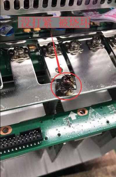
2. M10 chip pin function
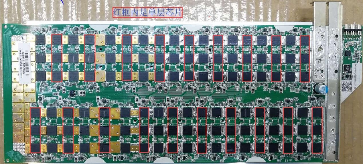
2.1. Single-layer chip pin function:
Chip: Pins 1, 20 are CLK;
Pins 4, 17 are RXD;
Pins 2, 19 are TXD;
Pins 3, 18 are CTS;
Pins 5, 16 are RST;
Pins 7, 14 are VDD IO power supply;
Pins 6, 15 It is powered by VDD PRE. Inside the red box is a single-layer chip (As shown below)
2.2. Dual-layer chip pin function:
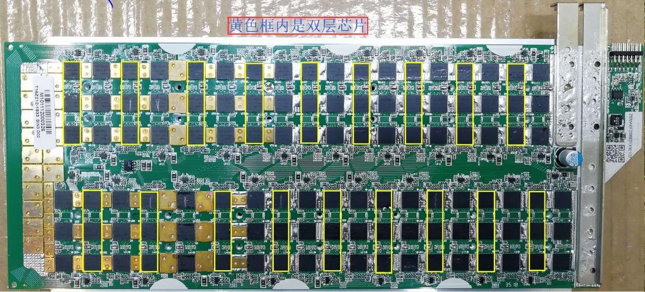
Chip:
Pins 5 and 16 are CLK;
Pins 4 and 17 are RXD;
Pins 2 and 19 are TXD;
Pins 3 and 18 are CTS;
Pins 1 and 20 are RST;
Pins 7 and 14 are VDD IO power supplies;
Pins 6 and 15 It is powered by VDD PRE. Inside the yellow box is a double-layer chip (As shown below).
3. M10 hash board signal process
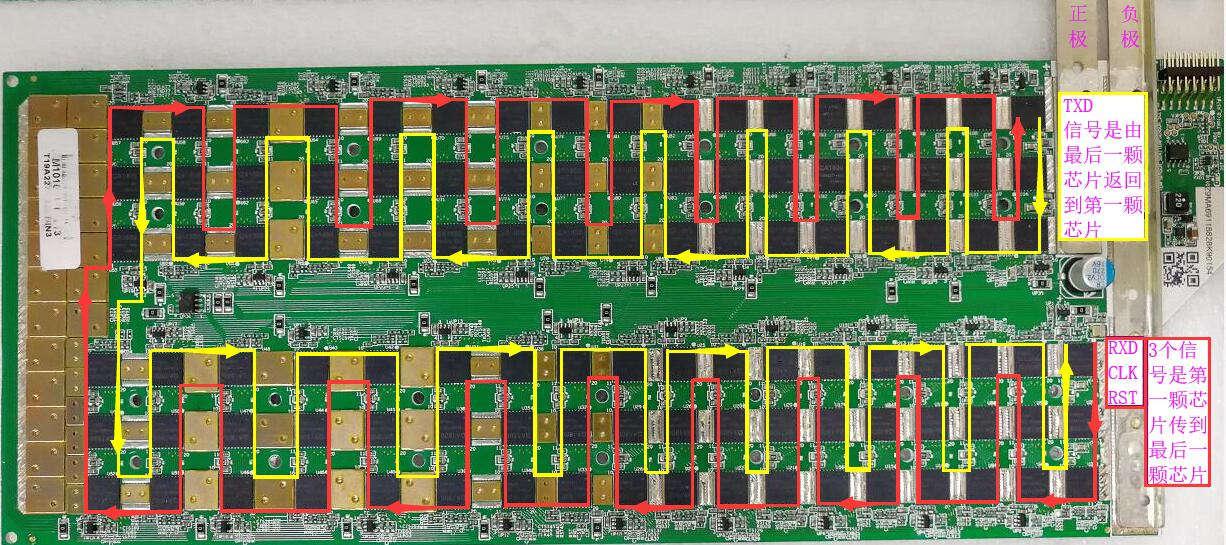
M10 is composed of 35 layers in series, each layer has 3 1800 chips in parallel, and the whole board has a total of 105 chips. Each layer of voltage domain has an independent LDO that provides 1.8v and 0.9v voltages and is composed of RST, CTS, RXD, TXD, and CLK. M10 has only 1 24M clock and 1 temperature sensor, plus 1 EEPROM is the whole board signal composition. Signal flow direction: CLK, RXD, RST are all transmitted from the first chip to the last chip, and TXD is returned from the last chip to the first chip.
4. Between layers of hash board Resistance and test points
4.1 Interlayer position and voltage value
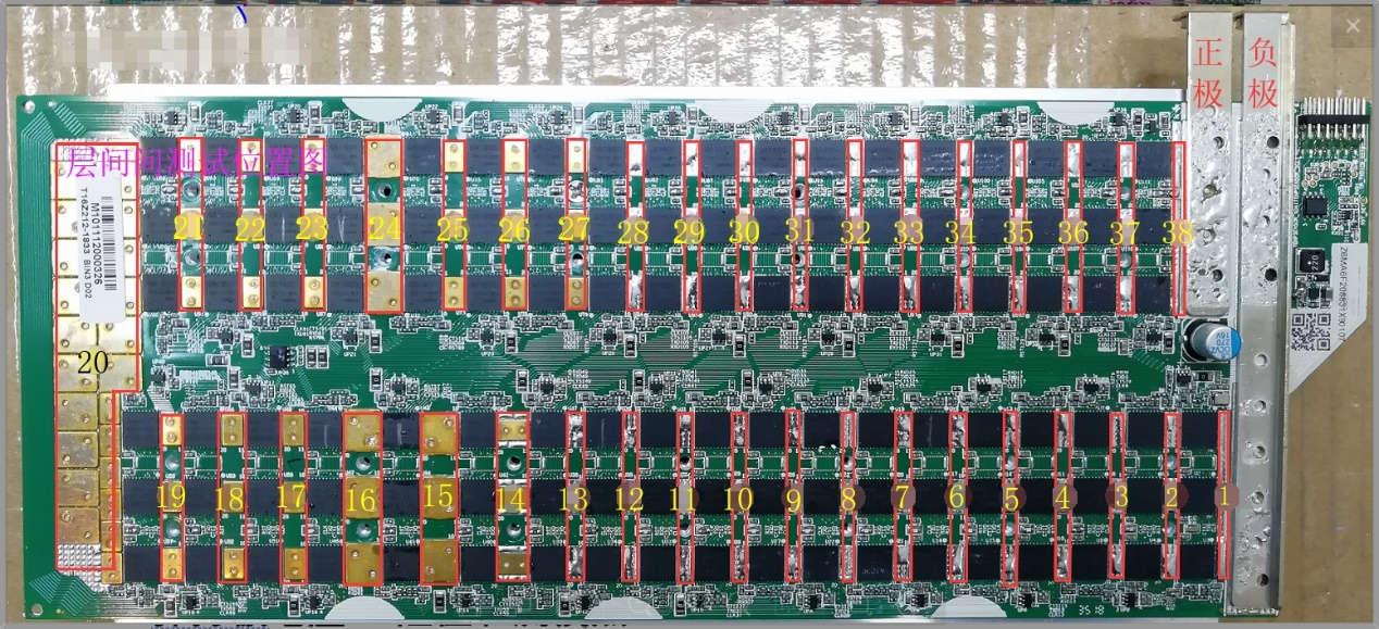
①The position of the layers is as shown in Figure 1 and 2 is the first layer, between 2 and 3 is the second layer, between 3 and 4 is the third layer, and so on for each layer.
②Interlayer voltage test position: layer 1 is the voltage value between 1 and 2, position 1 is the negative electrode of layer 1, and position 2 is the positive electrode of layer 1; layer 2 is the voltage value between layer 2 and 3, and position 2 is the negative electrode of layer 2. Position 3 is the positive electrode of layer 2; layer 3 is the voltage value between 3 and 4, position 3 is the negative electrode of layer 3, position 4 is the positive electrode of layer 3, and so on for each layer.
③The voltage value between layers is about 0 .34v.
4.2. Test points and values
①Each hash board has a corresponding test point and name. (As shown below)
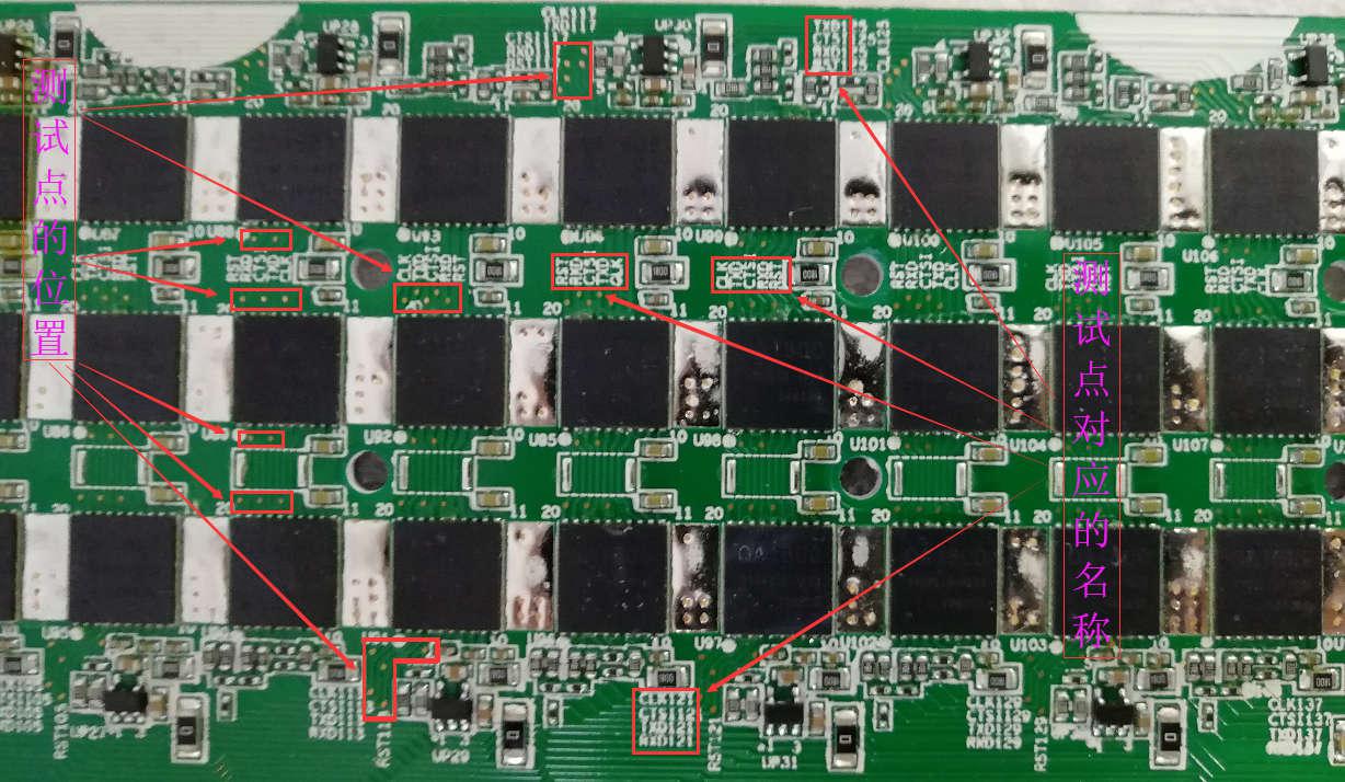
②The value of each point : CLK 1.8v±0.1v; RXT 1.8v; TXD 1.8v; RST pull high is 1.8v, pull low is 0v; IO 1.8v; PRE 0.8v±0.1v; the voltage between layers is about 0.35v.
Measured with diode files, CLK.RXD.TXD.RST.CTS is about 540Ω, IO is about 40Ω, and PRE is about 26Ω.
5. Repair case (Attention before maintenance: When powering on, the positive and negative poles of the power supply must not be reversed, and you need to check repeatedly before powering on!!!)
5.1. Prepare tools before repair
Preparation tools: oscilloscope, fluke 15b+ multimeter, power supply (Adjustable power supply above 10A) , Heating table, soldering iron with air gun, tweezers, flux, test control board, row Wire, solder, etc.
5.2. Testing method:
The first step: Remove the radiator, and visually check all the accessories of the power plate to see if there is any burning or tin bead phenomenon.
Step 2: Use the ohm file to measure the power input terminal of the force board. The normal value is about 6.5Ω. If there is a short circuit, it cannot be powered on. First remove the short circuit and then power on.
So as not to cause secondary damage.
Step 3: The power supply terminal resistance value of the hashrate board is normal, power-on test, test whether the reset is successful, and the reset is unsuccessful. Check the inter-layer voltage.
The fourth step: reset is normal, test whether chipid is PASSED If failed, check the CLK, TXD, RXD signals. Step 5: chipid test PASSED , Check the effective value of the chip when the hash rate is low.
5.3. Repair case:
Case 1: The chipid cannot be read in the power-on test, and the reset light does not light up.
Fault analysis: the reset light does not light up, use echo 0> /sys/class/gpio/gpio99/value and echo 1> /sys/class/gpio/gpio99/value command to test, it is true that the light does not light, the visual inspection light and other accessories are not Damaged, the interlayer voltage was further checked, and it was found that the interlayer voltage of layer 1 and layer 2 and 37 layers was only 0.2~0.26v. At this time, do not change the chips in a hurry. First, the chips between layers 1, 2, and 37 are interchanged, and the result is exchanged. Test the low inter-domain voltage on the first layer, and finally replace the first layer chip, and the test is OK.
Case 2: The reset is normal and the chipid cannot be read.
Fault analysis: the reset is normal and the chipid cannot be read. First check the CLK signal. The CLK signal voltage is about 1.8v. Check from layer 1 to the bottom layer. The measured u68 CLK is 1.8v, test the voltage between the layers of this layer is normal, determine the u68 chip problem, replace u68, test the chipid as PASSED.